Basic overview of ESD
Static electricity is caused by the mutual friction of two different substances, and a high voltage is formed by the accumulation of positive and negative charges in the two objects rubbing against each other. Man-made fibers and plastics are common triboelectric materials, and ESD problems arise when a voltage is generated by friction. For electronic components, electrostatic energy cannot be ignored, it can break down semiconductor components, thereby destroying electronic circuits.
Usually ESD creates EMC problems in two main ways: conduction and radiated interference.
(1) Conduction mode. Electrostatic discharge current flows directly through the circuit, because ESD generates a very high voltage. If it enters the semiconductor, it may cause misoperation and easily destroy the semiconductor device. The internal insulation of modern semiconductor components is often at a voltage of tens of volts. Breakdown and permanent short circuit, this is a very serious ESD problem, which is common in daily life.
(2) Radiation interference. When electrostatic discharge (can be simulated with an electrostatic discharge tester), the generated spark voltage will generate a radiated magnetic field and electric field. Magnetic fields can induce noise voltages in various signal loops in nearby circuits. Due to the large electrostatic current generated in a short period of time, the noise voltage generated in the signal loop may exceed the threshold level of the logic components, causing false triggering of the components.
In circuits, ESD problems caused by static electricity from the human body are the most common. The voltage of human ESD in dry climate environment can easily exceed 8kV, 15kV or even 20kV, so we need to pay attention to the impact of such electrostatic voltage on PCB and components, and take corresponding measures to prevent ESD problems.
Usually we can take insulation, shielding, isolation, filtering and other methods to protect the product.
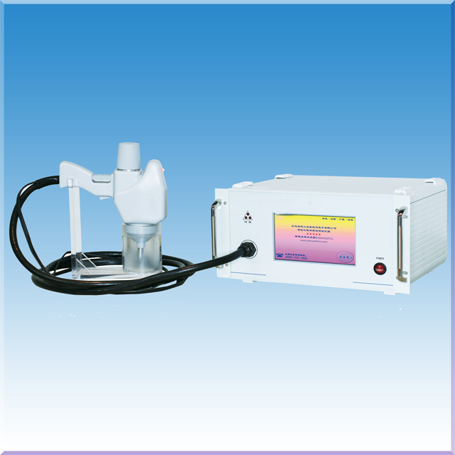
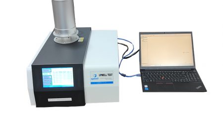
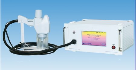
EN/IEC61000-4-2,ISO10605 EMC ESD Simulator
Electrostatic discharge protection design and measures
- Design principles to reduce the impact of ESD
There are many ways to reduce the EMI effects of ESD: completely preventing ESD from being generated, preventing EMI from coupling into the circuit or device, and increasing the inherent immunity of the device through the design process.
It is possible to control ESD in an environment that completely prevents ESD from occurring. But for the equipment in the field, the disturbance resistance of the system must be enhanced through the design process. A common design approach is to place protection circuits between hazardous points of the device, such as the input and ground, that only function when the ESD induced voltage exceeds the limit. They provide low-impedance switching channels through which system-stored charge can flow safely to ground. The protection circuit may include a plurality of current shunt units.
- Additional protection measures to reduce the impact of ESD
The design of the circuit should take into account that unrestricted wait or cut-off states are not allowed.
1) The unused input terminals in the device are not allowed to be disconnected or suspended.
2) The filter prevents ESD from coupling into the device. If the input is high impedance, a bypass capacitor filter is most effective because its low impedance will effectively bypass the high input impedance. The closer the bypass capacitor is to the input, the better. If the input impedance is low, using a ferrite inductance element in series with the circuit can provide better filtering, and these ferrite elements should also be as close to the input as possible.
3) PCB design plays an important role in improving the ESD anti-disturbance characteristics of the system. The traces on the PCB are the radiating antennas for EMI generated by ESD. In order to keep the coupling reduction lines of these antennas as short as possible, the enclosed area is as small as possible. At the same time, when the components are not evenly spread over the entire area of a large board, the common-mode coupling is enhanced. Using a multi-layer board or a ground grid to reduce the coupling can also suppress common-mode radiation noise.
4) Housing design is another key to preventing ESD radiation and conduction coupling.
5) A properly designed cable protection system may be the key to improving system insensitivity. As the largest antennas in most systems, input and output cables are particularly susceptible to EMI-induced large voltages or currents. On the other hand, the cable provides a low impedance path. Conducted coupling can be avoided if the shielded cable is reliably connected to the chassis ground. To reduce radiated EMI coupling to the cable, the wire length and loop area should be reduced. Common mode coupling should be suppressed and Use metal mesh shielding.
6) In addition to hardware measures, software EMI solutions are also an effective way to reduce serious malfunctions such as system lock-up.
The electromagnetic field energy generated by ESD can cause equipment malfunction or even damage. Electromagnetic noise (EMI) affects electronic equipment through conduction or radiation. The energy coupled to the integrated circuits in a device is proportional to the peak electric field and the conversion products of the electric field.